Вафля GaN эпитаксиальная
(69)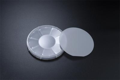
4-дюймовый легированный магнием GaN P-типа на сапфировой пластине SSP Удельное сопротивление ~ 10 Ом См Светодиодный лазер PIN Эпитаксиальная пластина
Цена: Negotiable
MOQ: Negotiable
Срок поставки: 3-4 week days
Бренд: GaNova
Выделять:LED Laser PIN Epitaxial Wafer
4-дюймовый GaN P-типа, легированный магнием, на сапфировой пластине Удельное сопротивление SSP ~ 10 Ом·см Светодиод, лазер, эпитаксиальная пластина PIN
Электрические свойства GaN p-типа, легированного Mg, исследуются посредством измерений эффекта Холла при переменной температуре.Образцы с диапаз... Посмотреть больше
Связаться сейчас
Fe дал допинг резистивности субстратов GaN > 10 ⁶ Ω·Приборы RF см
Цена: Negotiable
MOQ: Negotiable
Срок поставки: 3-4 week days
Бренд: GaNova
Выделять:ISO GaN Substrates, gan semiconductor wafer, Fe Doped GaN Substrates
2inch C-face Fe-doped SI-type free-standing GaN single crystal substrate Resistivity > 106 Ω·cm RF devices The achieved breakdown voltage of the Fe-doped GaN epitaxial layer can be as high as 2457 V, which is attributed to the Fe-doped GaN epitaxial layer with higher resistance, which can sustain... Посмотреть больше
Связаться сейчас
625um к 675um вафля СИД GaN 4 дюймов голубая эпитаксиальная на сапфире сапфира SSP плоском
Цена: Negotiable
MOQ: Negotiable
Срок поставки: 3-4 week days
Бренд: GaNova
Выделять:625um GaN Epitaxial Wafer, SSP gan on sapphire wafers, 675um GaN Epitaxial Wafer
Substrate Thickness 650 ± 25 μm 4 Inch Blue LED GaN Epitaxial Wafer On Sapphire SSP Flat Sapphire 4 inch Blue LED GaN epitaxial wafer on sapphire SSP For example, GaN is the substrate which makes violet (405 nm) laser diodes possible, without use of nonlinear optical frequency-doubling. Its sensitiv... Посмотреть больше
Связаться сейчас

2-дюймовый зеленый светодиод GaN на кремниевой пластине
Цена: Negotiable
MOQ: Negotiable
Срок поставки: 3-4 week days
Бренд: GaNova
Выделять:2 дюйма GaN на кремниевой пластинке, Зеленый светодиод GaN на кремниевой пластине, 520nm GaN на кремниевой пластине
2-дюймовый зеленый светодиод GaN на кремниевой пластине
Обзор
Нитрид галлия (GaN) создает инновационный сдвиг во всем мире силовой электроники.На протяжении десятилетий полевые МОП-транзисторы на основе кремния (металлооксидные полупроводниковые полевые транзисторы) были неотъемлемой частью пов... Посмотреть больше
Связаться сейчас
10 X 10,5 мм2 C Лицо Недопированный N Тип свободно стоящий GaN однокристаллический субстрат
Цена: Negotiable
MOQ: Negotiable
Срок поставки: 3-4 week days
Бренд: GaNova
Выделять:Недопированный однокристаллический субстрат GaN, Свободно стоящий субстрат GaN одиночного Кристл, N-тип однокристаллический субстрат GaN
C-сторона ² 10*10.5mm ООН-дала допинг n типа свободно стоящей резистивности субстрата GaN одиночной кристаллической < 0="">
Обзор
Наградные качественные субстраты GaN кристаллические с низкой плотностью дислокации (заказанн 105 /cm2) и поверхностью формы без периодических дефектов. Эти... Посмотреть больше
Связаться сейчас

10*10,5mm2 C-Face Fe-Doped SI-Type Free-Standing GaN Single Crystal Substrate Макродефект плотность 0cm−2 TTV ≤ 10 μm Сопротивление 106 Ω·Cm Устройства для радиочастотного облучения
Цена: Negotiable
MOQ: Negotiable
Срок поставки: 3-4 week days
Бренд: GaNova
Выделять:Субстрат GaN одиночный кристаллический, 10*10, 5mm2 GaN однокристаллическая субстрата
C-сторона 10*10.5mm2 Fe-дала допинг SI типа свободно стоящей резистивности субстрата GaN одиночной кристаллической > 106 Ω·вафля приборов RF см
Обзор
Мы продаем сразу от фабрики, и поэтому можем предложить самые лучшие цены на рынке для высококачественных субстратов GaN кристаллических. Кл... Посмотреть больше
Связаться сейчас
10 X 10,5 мм2 свободно стоящие субстраты GaN - 10 Мм ≤ BOW ≤ 10 Мм
Цена: Negotiable
MOQ: Negotiable
Срок поставки: 3-4 week days
Бренд: GaNova
Выделять:Свободные стоящие субстраты GaN, 10 x 10, 5 мм2 ГаН субстраты
10*10,5 мм² С-образная поверхность Нелегированная отдельно стоящая монокристаллическая подложка GaN n-типа Удельное сопротивление < 0,1 Ом·см Силовое устройство/лазер
Приложения
Лазерные диоды: фиолетовый LD, синий LD и зеленый LDСиловые электронные устройства, Высокочастотные электронные... Посмотреть больше
Связаться сейчас

TTV ≤ 10μm A-Face Un-Doped N-Type Free-Standing GaN Single Crystal Substrate Сопротивляемость 0,1 Ω·cm Мощное устройство/Лазер W
Цена: Negotiable
MOQ: Negotiable
Срок поставки: 3-4 week days
Бренд: GaNova
Выделять:Лазер W GaN однокристаллический субстрат, Силовое устройство GaN однокристаллическая подложка, Свободно стоящий однокристаллический субстрат GaN
-сторона 5*10mm2 ООН-дала допинг n типа свободно стоящей резистивности субстрата GaN одиночной кристаллической < 0="">
ОбзорНитрид галлия (GaN) очень трудный, механически стабилизированный широкий полупроводник bandgap. С более высокой пробивной напряженностью, более быстро переключая с... Посмотреть больше
Связаться сейчас

350 ± 25μm Толщина Недопированный свободно стоящий однокристаллический субстрат GaN N-типа с TTV ≤ 10μm и сопротивлением 0,1 Ω·cm
Цена: Negotiable
MOQ: Negotiable
Срок поставки: 3-4 week days
Бренд: GaNova
Выделять:10μm GaN однокристаллический субстрат, Субстрат GaN одиночный кристаллический
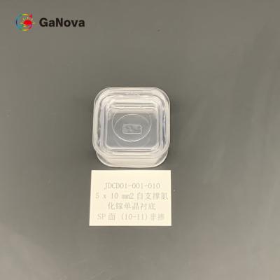
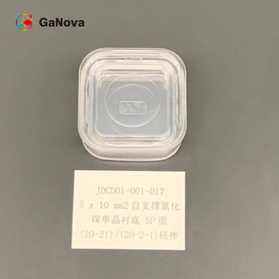
5*10mm2 SP-сторона (20-21)/(20-2-1) ООН-дал допинг n типа свободно стоящей резистивности субстрата GaN одиночной кристаллической < 0="">
ОбзорСубстрат нитрида галлия (GaN) высококачественный субстрат одно-Кристл. Он сделан с первоначальным методом HVPE и технологическим прочессом вафли,... Посмотреть больше
Связаться сейчас
5*10mm2 SP-Face 10-11 Недопированный N-тип свободно стоящий GaN однокристаллический субстрат 0,1 Ω·cm Сопротивляемость для силового устройства
Цена: Negotiable
MOQ: Negotiable
Срок поставки: 3-4 week days
Бренд: GaNova
Выделять:0.1 Ω·cm GaN однокристаллический субстрат, 5*10mm2 GaN однокристаллический субстрат
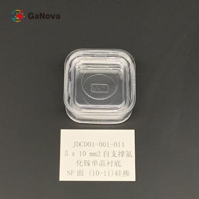
SP-сторона 5*10.5mm2 (10-11) ООН-дала допинг n типа свободно стоящей резистивности субстрата GaN одиночной кристаллической < 0="">
Генеративные враждебные сети (GANs) алгоритмические архитектуры которые используют 2 нервной системы, делая ямки одна против другого (таким образом «враждебн... Посмотреть больше
Связаться сейчас
5x10mm2 SP-Face 10-11 Недопированный N-тип свободностоящий однокристаллический субстрат GaN с TTV ≤ 10μm Сопротивляемость 0,05 Ω·cm
Цена: Negotiable
MOQ: Negotiable
Срок поставки: 3-4 week days
Бренд: GaNova
Выделять:Свободно стоящий субстрат GaN одиночного Кристл, 5x10mm2 GaN однокристаллический субстрат
SP-сторона 5*10mm2 (10-11) ООН-дала допинг n типа свободно стоящей резистивности субстрата GaN одиночной кристаллической < 0="">
ОбзорGaN имеет много серьезных преимуществ над кремнием, был больше привести эффективное, быстрое в действие, и даже лучше кривые восстановления. Однако, пока... Посмотреть больше
Связаться сейчас
Макродефект плотность 0cm−2 Недопированный SI-тип свободностоящий GaN однокристаллический субстрат для радиочастотных устройств 5*10mm2 M-Face
Цена: Negotiable
MOQ: Negotiable
Срок поставки: 3-4 week days
Бренд: GaNova
Выделять:Радиочастотные устройства GaN однокристаллическая подложка, 5*10mm2 GaN однокристаллический субстрат, Свободно стоящий однокристаллический субстрат GaN
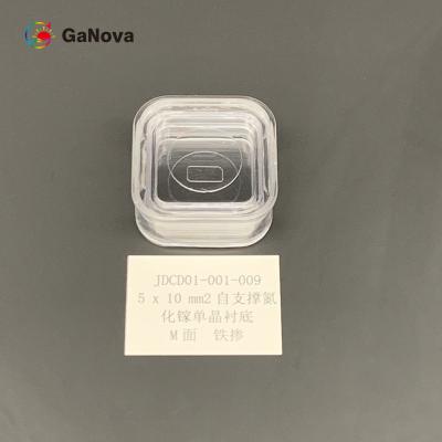
M-сторона 5*10mm2 ООН-дала допинг SI типа свободно стоящей резистивности субстрата GaN одиночной кристаллической > 106 Ω·вафля приборов RF см
ОбзорТонкие вафли Epi обыкновенно использованы для приборов MOS ведущей кромки. Толстое Epi или Мульти-наслоенные эпитаксиальные вафли использованы д... Посмотреть больше
Связаться сейчас

SP-Face 11-12 Недопированный N-тип свободностоящий GaN однокристаллический субстрат Сопротивляемость 0,05 Ω·cm Макродефект плотность 0cm−2
Цена: Negotiable
MOQ: Negotiable
Срок поставки: 3-4 week days
Бренд: GaNova
Выделять:00, 05 Ω·cm GaN однокристаллическая подложка, Недопированный однокристаллический субстрат GaN
5*10 мм2SP-face (11-12) Нелегированная отдельно стоящая монокристаллическая подложка GaN n-типа Удельное сопротивление < 0,05 Ом·см Силовое устройство/лазерная пластина
ОбзорПоскольку транзисторы GaN могут включаться быстрее, чем кремниевые транзисторы, они могут уменьшить потери, вызванные ... Посмотреть больше
Связаться сейчас

Устройство питания 5x10mm2 Недопированный N-тип свободно стоящий однокристаллический субстрат GaN с сопротивлением 0,1 Ω·cm и BOW в пределах 10μm
Цена: Negotiable
MOQ: Negotiable
Срок поставки: 3-4 week days
Бренд: GaNova
Выделять:0.1 Ω·cm GaN однокристаллический субстрат, 10μm GaN однокристаллический субстрат, 5x10mm2 GaN однокристаллический субстрат
SP-сторона 5*10mm2 (11-12) ООН-дала допинг n типа свободно стоящей резистивности субстрата GaN одиночной кристаллической < 0="">
ОбзорС 1990s, оно было использовано обыкновенно в светоизлучающих диодах (СИД). Нитрид галлия дает с голубого света используемого для диск-чтения в Blu-ray. Д... Посмотреть больше
Связаться сейчас
5*10mm2 SP-Face Un-Doped N-Type Free-Standing GaN Single Crystal Substrate 20-21 / 20-2-1 10mm2 Сопротивляемость 0,05 Ω·cm
Цена: Negotiable
MOQ: Negotiable
Срок поставки: 3-4 week days
Бренд: GaNova
Выделять:00, 05 Ω·cm GaN однокристаллическая подложка, 10mm2 GaN однокристаллический субстрат, 20-21 GaN однокристаллическая субстрата
5*10mm2 SP-сторона (20-21)/(20-2-1) ООН-дал допинг n типа свободно стоящей резистивности субстрата GaN одиночной кристаллической < 0="">
ОбзорГенеративная враждебная сеть (GAN) имеет 2 части: Генератор учит произвести правдоподобные данные. Произведенные примеры будут отрицательными тре... Посмотреть больше
Связаться сейчас
Размер 520±10nm 2inch ВЕДОМОЕ Зелен GaN на слое кремниевой пластины 20nmContact
Цена: Negotiable
MOQ: Negotiable
Срок поставки: 3-4 week days
Бренд: GaNova
Выделять:20nm GaN On Silicon Wafer, 520±10nm GaN On Silicon Wafer
2inch ВЕДОМОЕ Зелен GaN на кремниевой пластине
Обзор
Нитрид галлия (GaN) создает новаторский перенос повсеместно в мир производительности электроники. На десятилетия, основанные на кремни MOSFETs (транзисторы влияния поля полупроводника металлической окиси) неотъемлемая часть ежедневного совр... Посмотреть больше
Связаться сейчас

2inch ВЕДОМОЕ Сине GaN на лазере 455±10nm D'Onde Longueur кремниевой пластины
Цена: Negotiable
MOQ: Negotiable
Срок поставки: 3-4 week days
Бренд: GaNova
Выделять:455±10nm GaN On Silicon Wafer
2inch ВЕДОМОЕ Сине GaN на кремниевой пластине
Нитрид галлия полупроводниковые технологии используемые для наивысшей мощности, высокочастотных применений полупроводника. Нитрид галлия показывает несколько характеристик которые делают его лучшим чем GaAs и кремний для различных компонентов на... Посмотреть больше
Связаться сейчас

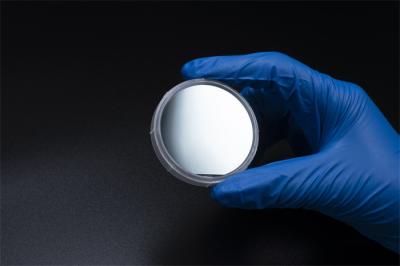
2-дюймовая C-образная поверхность, легированная Fe, отдельно стоящая монокристаллическая подложка GaN типа SI Удельное сопротивление > 10⁶ Ом·см РЧ-устройства
Цена: Negotiable
MOQ: Negotiable
Срок поставки: 3-4 week days
Бренд: Nanowin
Выделять:2inch GaN Single Crystal Substrate, Resistivity GaN Single Crystal Substrate
2-дюймовая отдельно стоящая монокристаллическая подложка GaN типа SI с С-образной поверхностью, легированная Fe Удельное сопротивление > 106Ом·см РЧ-устройства
Обзор
Эпитаксиальные пластины нитрида галлия (GaN) (эпи-пластины).Пластины GaN-транзисторов с высокой подвижностью электронов (HEMT) ... Посмотреть больше
Связаться сейчас

Mg-данная допинг 4-Inch вафля PIN лазера СИД см субстратов SSP Resistivity~10Ω GaN/сапфира эпитаксиальная
Цена: Negotiable
MOQ: Negotiable
Срок поставки: 3-4 week days
Бренд: GaNova
Выделять:LED Laser GaN Epitaxial Wafer
4 дюйма P типа Mg-данное допинг GaN на СИД см вафли SSP resistivity~10Ω сапфира, лазере, вафле PIN эпитаксиальной
Почему используйте вафли GaN?
Нитрид галлия на сапфире идеальный материал для амплификации энергии радио. Он предлагает несколько преимуществ над кремнием, включая более высоко... Посмотреть больше
Связаться сейчас
4-дюймовый легированный UID GaN N-типа на сапфировой пластине SSP Удельное сопротивление > 0,5 Ом·см Светодиод, лазер, эпитаксиальная пластина PIN
Цена: Negotiable
MOQ: Negotiable
Срок поставки: 3-4 week days
Бренд: GaNova
Выделять:PIN GaN On Sapphire Wafer, 4 Inch GaN On Sapphire Wafer
4-дюймовый GaN, легированный UID N-типа, на сапфировой пластине Удельное сопротивление SSP > 0,5 Ом·см Светодиод, лазер, эпитаксиальная пластина PIN
Например, GaN является подложкой, которая делает возможными фиолетовые (405 нм) лазерные диоды без использования нелинейного оптического удвоени... Посмотреть больше
Связаться сейчас